STMicroelectronics TSZ901 High Accuracy/Bandwidth Zero Drift Op Amps
STMicroelectronics TSZ901 High Accuracy/Bandwidth Zero Drift Operational Amplifiers (Op Amps) are designed for precision applications requiring long-term stability and low noise. Featuring an ultra-low input offset voltage of just 3µV (maximum) and near-zero drift over temperature and time, the STMicro TSZ901 ensures consistent performance in demanding environments. The op amps offer a high bandwidth of 10MHz and a low input bias current of 200pA, making the devices ideal for sensor signal conditioning, medical instrumentation, and industrial control systems. Operating from a single supply voltage as low as 1.8V, the TSZ901 is well-suited for low-power designs, while rail-to-rail input and output architecture maximizes the dynamic range. With robust ESD protection and a compact footprint, the TSZ901 op amps deliver precision and reliability in space-constrained applications.
Features
- Ultra-high accuracy and stability
- 5μV maximum offset voltage at +25°C
- 8μV offset voltage over the full temperature range (-40°C to +125°C)
- Rail-to-rail input/output
- Low 2.5V to 5.5V supply voltage range
- Low 1.5mA power consumption at 5V
- 10MHz gain-bandwidth product
- AEC-Q100 automotive qualification
- Extended -40°C to +125°C temperature range
- Higher accuracy without calibration
- Accuracy is virtually unaffected by temperature change
- RoHS compliant
Applications
- High-accuracy signal conditioning
- Automotive current measurement and sensor signal conditioning
Specifications
- 6V maximum supply voltage
- ±10mA maximum input current
- ±8µV maximum input offset voltage
- ±30nV/°C maximum input offset voltage drift over temperature
- 200pA to 300pA typical input bias/offset current range
- 135dB typical open-loop gain
- 122dB typical common-mode rejection ratio
- 140dB typical supply-voltage rejection ratio
- 50mV to 70mV maximum high-/low-level output voltage drop
- 50mA typical source/sink
- 2.0mA maximum supply current (per op amp)
- 6V/µs typical slew rate
- 50° typical gain margin
- 9nV/√Hz typical input voltage noise density
- 0.2µVpp typical input noise voltage
- 2µs typical overload recovery time
- 1µs typical settling time
- 84dB to 91dB typical EMI rejection rate range
- +150°C maximum junction temperature
- 250°C/W maximum thermal resistance
- Maximum ESD ratings
- 4kV Human Body Model (HBM), industrial and automotive grade
- 1kV Charged-Device Model (CDM)
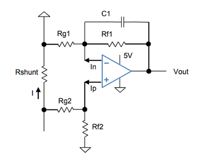
Low-Side Current Sensing Schematic


