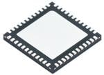
LMK00301ARHST

Texas Instruments
595-LMK00301ARHST
LMK00301ARHST

Mfr.:

Description:
Clock Buffer 3-GHz 10-output dif ferential fanout buf A 595-LMK00301ARHSR

ECAD Model:
Download the free Library Loader to convert this file for your ECAD Tool. Learn more about ECAD Model.

In Stock: 413

Stock:
413 Can Ship Immediately
Factory Lead-Time:
6 Weeks Estimated factory production time for quantities greater than shown.
Minimum: 1   Multiples: 1
Unit Price:
$-.--
Ext. Price:
$-.--
Est. Tariff:
Packaging:
Full Reel (Order in multiples of 250)

Pricing (CAD)

Qty. Unit Price
Ext. Price
Cut Tape / MouseReel™
$17.15 $17.15
$13.43 $134.30
$12.49 $312.25
$11.48 $1,148.00
Full Reel (Order in multiples of 250)
$10.98 $2,745.00
$10.53 $5,265.00
$10.38 $10,380.00
2,500 Quote
† $8.50 MouseReel™ fee will be added and calculated in your shopping cart. All MouseReel™ orders are non-cancellable and non-returnable.

Product Attribute Attribute Value Select Attribute
Texas Instruments
Product Category: Clock Buffer
RoHS:  
10 Output
3.1 GHz
2.3 ns
LVPECL, LVDS, HCSL, LVCMOS
WQFN-48
LVPECL, LVDS, CML, SSTL, HSTL, HCSL
3.1 GHz
3.15 V
3.45 V
LMK00301
- 40 C
+ 85 C
Brand: Texas Instruments
Duty Cycle - Max: 55 %
Moisture Sensitive: Yes
Mounting Style: SMD/SMT
Operating Supply Current: 20 mA
Packaging: Reel
Packaging: Cut Tape
Packaging: MouseReel
Product: Fanout Buffers / Level Translators
Product Type: Clock Buffers
Factory Pack Quantity: 250
Subcategory: Clock & Timer ICs
Type: Differential Clock Buffer/ Level Translator
Unit Weight: 143.600 mg
Products found:
To show similar products, select at least one checkbox
Select at least one checkbox above to show similar products in this category.
Attributes selected: 0

This functionality requires JavaScript to be enabled.

CAHTS:
8542390000
CNHTS:
8542399000
USHTS:
8542390090
MXHTS:
8542399999
ECCN:
EAR99

LMK00301 Fanout Buffer / Level Translator

Texas Instruments LMK00301 Differential Fanout Buffer / Level Translator is a 3GHz, 10-output differential fanout buffer intended for high-frequency, low-jitter clock/data distribution and level translation. The input clock is selected from two universal inputs or one crystal input. The selected input clock is distributed to two banks of 5 differential outputs and one LVCMOS output. Both differential output banks can be independently configured as LVPECL, LVDS, or HCSL drivers or disabled. The LVCMOS output has a synchronous enable input for runt-pulse-free operation when enabled or disabled. The LMK00301 operates from a 3.3V core supply and 3 independent 3.3V/2.5V output supplies.